

As artificial intelligence, high-performance computing, and data-intensive technologies continue to push conventional semiconductor technology toward its physical limits, innovators around the world are searching for the next breakthrough in computing. Among them is Dr. Ko-Cheng Fang, Founder and CEO of LongServing Technology, who has introduced an ambitious architectural concept designed to redefine how information is processed—using light instead of electricity.
On April 23, 2026, LongServing Technology publicly unveiled three key architectural designs that offer its most comprehensive look yet at the company’s proposed photonic computing platform. The release includes a three-dimensional chip architecture, a complete photonic pathway system, and a structural demonstration of a photonic full-adder—the fundamental computational building block of digital processors. According to the company, all three designs were personally created by Dr. Fang and represent years of research dedicated to advancing all-optical computing.

Unlike traditional semiconductor chips that move electrons through microscopic copper interconnects, LongServing Technology’s proposed architecture relies entirely on photons to transmit and process information. By replacing electrical pathways with optical ones, the company aims to eliminate many of the limitations associated with heat generation, signal resistance, and memory-transfer bottlenecks that increasingly challenge modern electronic processors.
One of the most distinctive features of the newly disclosed design is its 45-degree optical pathway architecture. Rather than following the conventional horizontal routing found in electronic integrated circuits, the company has redesigned the internal optical network with diagonal pathways intended to optimize the movement of light across the chip. This architectural shift reflects LongServing Technology’s vision of building computing systems specifically for photonic operation instead of adapting existing electronic designs.
The newly released designs also introduce a three-layer structural architecture, representing a departure from the multi-layer manufacturing processes commonly used in electronic semiconductor fabrication.
According to the company, the proposed structure consists of:
- A bottom layer dedicated to photonic memory, designed to store information entirely within the optical domain.
- A middle layer containing photonic logic gates, where computational operations are performed.
- A top layer composed of photonic pathways, enabling optical signals to travel throughout the processor.
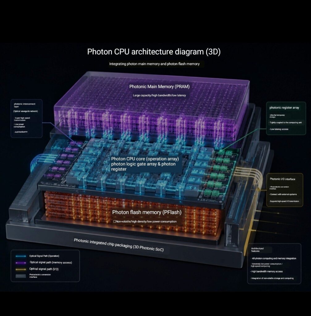
Each layer is intended to be fabricated using its own dedicated photomask, creating an integrated optical computing platform. LongServing Technology believes this architecture could simplify fabrication compared with conventional electronic chips while enabling closer integration between memory, computation, and data transmission.
Another highlight of the announcement is the first public demonstration of the company’s photonic full-adder architecture. As one of the most fundamental elements in digital computing, a full adder performs binary arithmetic that underpins virtually every modern processor. By demonstrating how this function could be implemented through optical circuitry, the company seeks to illustrate the potential foundation for future generations of entirely photonic processors.

A central element of LongServing Technology’s vision is the integration of photonic memory directly into the processor architecture. Traditional computer systems separate processing units from memory, requiring continuous movement of data between the two—a constraint widely recognized as one of the primary performance limitations in modern computing.
The company proposes that by integrating memory directly within an all-optical architecture, information can remain inside the photonic environment throughout computation, reducing latency while minimizing the need for repeated electrical-to-optical signal conversion.
According to LongServing Technology, this integrated approach has the potential to deliver computational performance measured in hundreds of thousands of times faster than conventional electronic chips. The company further notes that because optical signals travel at the speed of light, the theoretical upper limits of such architectures remain difficult to quantify.
Beyond its technical ambitions, the public release of these architectural designs reflects an effort to provide greater visibility into the company’s research direction. Rather than presenting only conceptual descriptions, LongServing Technology has shared structural illustrations that communicate how its proposed photonic platform is intended to function, offering engineers, researchers, investors, and technology observers a clearer understanding of its long-term vision.

As demand continues to accelerate for artificial intelligence infrastructure, cloud computing, autonomous systems, and next-generation data centers, researchers worldwide are exploring alternatives to traditional silicon-based computing. Photonic computing has emerged as one of several promising directions capable of supporting dramatically higher data throughput and greater energy efficiency.
Within this rapidly evolving landscape, Dr. Ko-Cheng Fang’s architectural concepts represent an ambitious contribution to the future of optical computing. While further engineering development, manufacturing advances, and independent validation will ultimately determine the commercial realization of these designs, the publication of the company’s photonic chip architecture marks a significant milestone in its ongoing research journey.
Whether viewed as a bold technological vision or the foundation of a future computing platform, LongServing Technology’s latest disclosure underscores a broader industry trend: the search for computing architectures capable of moving beyond the limitations of electrons and harnessing the extraordinary potential of light.












+ There are no comments
Add yours